
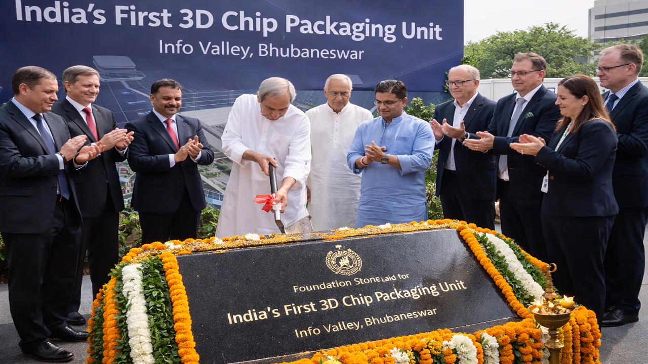
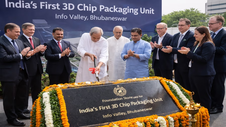
Odisha has made a giant stride in the semiconductor leg of India by laying the foundation stone of the country’s first futuristic 3D chip packaging unit at Info Valley, Bhubaneswar. The project being set up by 3D Glass Solutions through its Indian arm, Heterogeneous Integration Packaging Solutions Pvt. Ltd., will boost the country‘s semiconductor ecosystem.
ALSO READ- India’s GDP Rank Drops from 4th to 6th Position: IMF Reports
Historic Step for Odisha-
This new plant will surely turn over a new leaf for Odisha as well as India. According to the state‘s Chief Minister Mohan Charan Majhi, the project will be a “historic milestone” for the country, as, for the first time, high-end semiconductor packaging will be established in India at this scale. This will also position Odisha to be in a key position for Prime Minister Narendra Modi‘s mission for “Manufacturing India to become self-reliant in semiconductors & electronics manufacturing”.
With a sense of optimism, the largest companies in high technology, like Intel, Lockheed Martin, and Applied Materials, have reportedly tapped into advanced packaging products, and their great faith in Odisha was emphasised by the emerging profile of the state.
Why the Project Matters-
This is not another industrial project investment. Instead, the plant has been conceptualised as a strategic technology platform for the high-growth sectors like AI, high-performance computing, 5/6 G telecoms, defence electronics, aerospace/photonic/auto radar, and so on. Hence, this project is likely to boost India’s wider technology supply chain now that advanced chip packaging has assumed significant global manufacturing significance.
This project is equally important as it makes Odisha the only state in the country where both India’s first compound semiconductor fabrication unit and first 3D glass substrate packaging plant are coming up. That was until recently considered a huge advantage in creating a complete semiconductor ecosystem in a state.
Investment and Production Plan-
Total project investment of Rs 1,943.53 crore (including 799 crore Central fiscal support and about 399.5 crore of further State support). To set up a green field, HV, vertically integrated advanced packaging and embedded glass substrate ATMP facility.
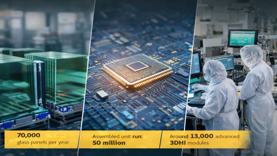
According to the announcement, the unit is expected to manufacture:
- 70,000 glass panels per year.
- Assembled unit run: 50 million.
- Officially, around 13,000 modules of advanced 3DHI.
- Commercial production should be achieved by August 2028, and volume production on a full scale should be achieved by August 2030.
Industry and Job Opportunities-
The state government said that the semiconductor ecosystem would generate a large number of employment opportunities for all engineering graduates, diploma holders, and ITI students. This was most needed for a state struggling to move away from a resource-based economy to one that is technology-driven.
Furthermore, the project could foster subsequent investments across a range of related areas, including electronics manufacturing, intelligent-enabled systems and advanced digital infrastructure. If the project achieves its planned goals, Odisha could emerge as a premier location for high-value manufacturing in eastern India.
Vaishnaw Highlights National Development-
Union Minister Ashwini Vaishnaw stated that under Prime Minister Narendra Modi, Odisha has been fast-growing as one of the most promising contributors to India’s semiconductor transformation. While Odisha is worldwide famous for its minerals, metals and energy sector, it is steadily acquiring momentum in electronics, IT and semiconductors.
He certainly alluded to India‘s wider electronics growth, as he said: Electronics production has increased six-fold in the last 12 years. India has become the second-largest producer of mobile phones in the world, and in 2025 was going to be the most significant exporter of mobile phones.
Rail Push Supports Growth-
Alongside the semiconductor announcement, Vaishnaw mentioned that large-scale rail infrastructure work is underway in Odisha. Projects with a cost of more than 90,000 crore are being executed in the state, and the state has been allotted a railway budget of 10,928 crore. He said the redevelopment of 59 stations is taking place under the Amrit Bharat Station Scheme, while all 30 districts are being connected through planned interventions.
A four-line coastal rail corridor from Balasore (north) to Berhampur(south), the other for feeding into the other, was also proposed in the overall plan for the development of connectivity. These enhancements would help in easing freight movement, enhancing passenger comfort and developing the region.
Policy Support and Skill Building-
State Electronics and IT Minister, Dr Mukesh Mahaling, said trends indicate the state is fast emerging as a semiconductor hub as the Government has recently formulated its IT, AI, GCC and Semiconductor Policies 2025. He said we are providing stipend support for Engineering students to help in creating a market-ready workforce.
He further connected the project to the Odisha mega project envisaged in future portals like the Blackswan Summit 2026 and the spike in AI investment flowing into the state. All these steps aim to bring in talent, develop skills and sharpen the state‘s focus on high-end technology zones.
Key Project Benefits-
The project is expected to deliver several long-term benefits:
- Enhanced global presence.
- More support to the following industries:
- AI
- 5G
- Air defense and aerospace
- Provide more job opportunities for youth with high and medium technical skills.
- Naik’s assurances to build investor confidence in Odisha.
- A larger share of global chip packaging for India.

ALSO READ- Claude Opus 4.7 Debuts With Stronger Coding Tools
Conclusion-
The first state-of-the-art 3D semiconductor packaging plant in Odisha is, in reality, being viewed as much more than just an industrial project. Experts see it as a symbol of India’s next phase of manufacturing, with heavy government support and global connections in technologies and policies that are likely to help Odisha become one of the key state-of-the-art semiconductor hubs in the future. If the plan is successfully implemented, Odisha might stand out as one of the crucial nodes in India’s quest to build its electronics and chip manufacturing industry.
FAQs-
A. The construction of India‘s first fully equipped 3D semiconductor packaging facility at Info Valley, Bhubaneswar.
A. The project is being carried out by 3D Glass Solutions Inc. through its Indian subsidiary Heterogeneous Integration Packaging Solutions Pvt. Ltd.
A. Total investment, including Central and State support, is 1943.53 crore.
A. It facilities for AI, 5G/6G, defence electronics, aerospace, photonics, automotive radar and data centres.
A. Commercial production planned for August 2028, with mass production by August 2030.
A. It enhances the domestic semiconductor capabilities and is helping the country in catering to its needs of self-sufficient electronics manufacturing.