
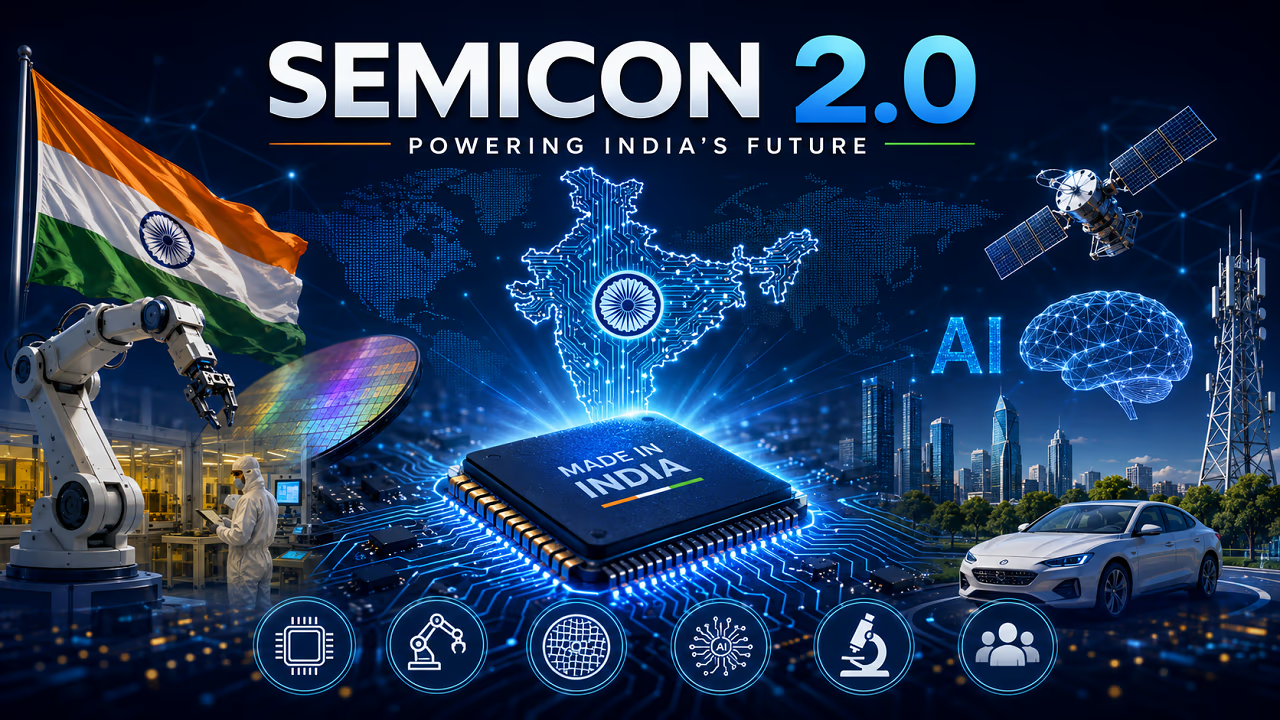
India has taken the most crucial decision in the domain of technology policies with the approval for India Semiconductor Mission (ISM) 2.0, also commonly referred to as Semicon 2.0. The initiative was greenlit in July 2026 by the Union Cabinet and is the most ambitious program of semiconductors, with an allocation of ₹1.27 lakh crore for 12 projects. With the mission shifting focus from just setting up factories for semiconductor production to a comprehensive value chain that includes all aspects of semiconductors, such as raw material procurement, manufacture of equipment, design, research and development, along with the availability of trained manpower and a resilient supply chain, it is indeed one of the most visionary plans.
ALSO READ- Village Telecom Survey: India’s Largest Rural Mobile Network Performance Survey
What is Semicon 2.0?
Semicon 2.0, also called India Semiconductor Mission (ISM) 2.0, represents the second phase of the semiconductor growth roadmap of India. The Semicon 1.0 semiconductors involved efforts at promoting fabrication, assembly and packaging through incentives; the second phase looks to develop an entire semiconductor ecosystem. It intends to make sure that apart from being a manufacturer of semiconductor chips, India also designs, tests, packages and supplies components that are crucial for the global semiconductor industry. The government is pushing for 12 semiconductor manufacturing projects in which large companies like Kaynes, Micron and CG Semi have already kicked off the production of products like a silicon fabrication (wafer fab), a silicon carbide fabrication, an integrated gallium nitride micro-LED display fab, and nine packaging plants. In terms of design, 24 projects of startups and MSMEs were granted funds for developing chips for artificial intelligence, satellite communications, Internet of Things (IoT), telecom, drones, cybersecurity, smart metering, and automotive electronic systems. Unlike the previous mission that sought to promote semiconductor chip manufacturing alone, ISM 2.0 seeks to offer assistance to:
- Manufacturing of semiconductor equipment
- Chemicals and materials for semiconductors
- Chip design and Indian Intellectual Property (IP)
- R&D-Research & Development centres
- Resilient supply chain
- Developing talent and advanced training centres
Semicon India 2026-
Under the guidance of Prime Minister Narendra Modi, India Semiconductor Mission (ISM), in collaboration with SEMI and associated industries, will be organising Semicon India 2026 from September 17 to September 19 2026. The Semicon India 2026 event will be organised in New Delhi(India) at Yashobhoomi India-International Convention & Expo Centre based on the theme “Building Trusted and Resilient Semiconductor Ecosystems”. The event aims to establish India as a trusted partner in the global value chain of the semiconductor industry. Technologies like AI, IoT, 5G/6G Communications, Electric Vehicles, Quantum Computing, Robotics, Aerospace, Defence Electronics, Computing, and Intelligent Manufacturing will benefit from this initiative.
Why the Need for Semicon 2.0?
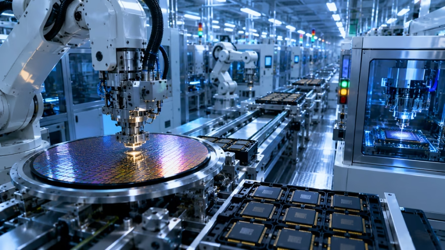
The emergence of Semicon 2.0 indicates India’s major transformation from an importer of semiconductors to a global supplier of semiconductor technology. However, the first phase of semiconductors (Semicon 1.0) has shown favourable outcomes, but the areas that were not achieved will be advanced in the second phase of the semiconductor mission.
- Growing Demand for Semiconductors across the World: Semiconductors are crucial for electronic and mobility products such as phones, laptops, EVs, AI, data centres, 5G networks, healthcare, defence, and aerospace. As the demand for state-of-the-art semiconductors is rising, there must be a strong indigenous system in place to fulfil not only India’s demands but also global demands.
- Lowering Dependency on Imported Chips: India imports many of the semiconductors that are used in the electronics and manufacturing sectors, thus increasing production costs and making the economy vulnerable. Moreover, during COVID-19, the country’s electronic and automobile industries faced a shortage of chips. With Semicon 2.0, India will domestically produce and fulfil the requirements.
- Moving Beyond Fabrication Plants: Semicon 1.0 focused primarily on setting up semiconductor and packaging plants; however, policymakers understood that, beyond fabrication plant setup, many other factors, such as semiconductor-grade raw materials, specific machinery, research, chip design, human resources, and robust supply chains, were necessary for a healthy semiconductor industry.
- Global Semiconductor Value Chain: India’s large base of engineers, a burgeoning electronics industry, and favourable government policies have the chance to be a valued global partner in semiconductor manufacturing and innovations.
- Boosting India’s Strategic and Digital Objectives: Government programs like Digital India, Make in India, Atmanirbhar Bharat, and the fast-emerging fields of artificial intelligence, electric mobility, and advanced electronics need a robust indigenous semiconductor value chain like Semicon 2.0 for meeting national objectives.
Six Pillars of Semicon 2.0-
For making India a global semiconductor player, Semicon 2.0 relies on six pillars strategically. By adopting a holistic approach, the Semicon 2.0 will cover the value chain: design to manufacturing, research, logistics, and even talent development:
- Advanced Semiconductor Fabs:
Wafer fabrication is the first pillar of Semicon 2.0, establishing semiconductor fabrication plants in India. These modern fabrication plants manufacture silicon wafers that are turned into semiconductors used in phones, computers, vehicles, consumer goods, industrial machinery, and even military equipment. By offering financial aid, the government tries to attract domestic and international companies for collaboration.
- Assembly, Testing, Marking and Packaging (ATMP/OSAT):
The second pillar is assembling, testing, packaging, and marking the chips. It plans to enhance India’s ATMP-Assembly, Testing, Marking and Packaging and OSAT-Outsourced Semiconductor Assembly and Test competencies to become a major centre for back-end semiconductor manufacturing and create large employment opportunities.
- Semiconductor Equipment and Materials Ecosystem:
The third pillar is building a local ecosystem of semiconductor equipment and material providers. Semiconductor manufacturing involves the use of very specialised machinery, silicon wafers, semiconductor-grade chemicals, speciality gases, photoresist, among other materials that India currently imports from abroad. One of the objectives of the initiative is to ensure local availability of all such inputs.
- Chip Design and Indigenous Intellectual Property (IP):
India has many semiconductor designers in its workforce who work for global IT firms. One of the key objectives of Semicon 2.0 is to capitalise on this strength and develop chip designs and indigenous IP through Electronic Design Automation (EDA), fabless semiconductor companies and indigenous design, among others.
- Research, Development and Innovation:
Innovation is crucial for the semiconductor sector in view of its constantly changing nature. This pillar focuses on industry-driven facilities that will foster industry-academic collaboration and the development of next-gen semiconductor technologies. The innovation in R&D will ensure advanced chip architecture, more materials, and enhanced production quality and technologies. Investment in this area will allow the country to stay competitive with respect to future semiconductor technologies.
- Skilled Workforce and Resilient Supply Chains:
The successful ecosystem of the semiconductor industry implies the presence of highly skilled engineers, technicians, scientists and supply chain experts. Semicon 2.0 places great stress on the preparation of the future-ready workforce via targeted education and training and semiconductor-related academic programs. Simultaneously, the initiative plans to create resilient supply chains via the enhancement of domestic capacity and international partnerships.
How Are the Features of Semicon 2.0 Better Than Those of Semicon 1.0?
| Feature | Semicon 1.0 | Semicon 2.0 |
| Primary focus | Establish semiconductor manufacturing | Build a complete semiconductor ecosystem |
| Chip fabrication | It has chip fabrication. | It has chip fabrication. |
| Packaging & testing | It consists of a simple packaging and testing system. | It consists of an advanced packaging and testing system. |
| Equipment manufacturing | Limited equipment is manufactured. | The major focus is on optimal equipment manufacturing. |
| Semiconductor materials | Limited materials are used in this. | Dedicated support for the supply of materials. |
| Design IP | Basic IP framework | Strong emphasis on indigenous IP |
| Research & Development | Limited research and development sources | Dedicated R&D centres |
| Supply chain | Partial supply | Comprehensive ecosystem approach |
| Talent development | Moderate-level talent acquisition | Industry-led research and skill centres |
| Budget | ₹76,000 crore (approx.) | ₹1.27 lakh crore |
Benefits of Semicon 2.0 for India-
- Economic Growth Enhancement: Semicon 2.0 is likely to make a great contribution to the growth of the Indian economy through attracting substantial investments from local and foreign sources to produce semiconductors.
- Creation of High-Paying Employment: Thousands of high-quality jobs for skilled workers, engineers, scientists, technicians, and professionals will be created in fields such as semiconductor production, chip designing, testing, packaging, and research. Indirect employment in allied industries will also be created.
- Fostering Innovation and Start-ups: By focusing on chip designing, research, and developing native semiconductor IP, Semicon 2.0 will promote innovations, start-ups, and development of next-generation semiconductor technology among MSMEs, start-ups, and academic institutions.
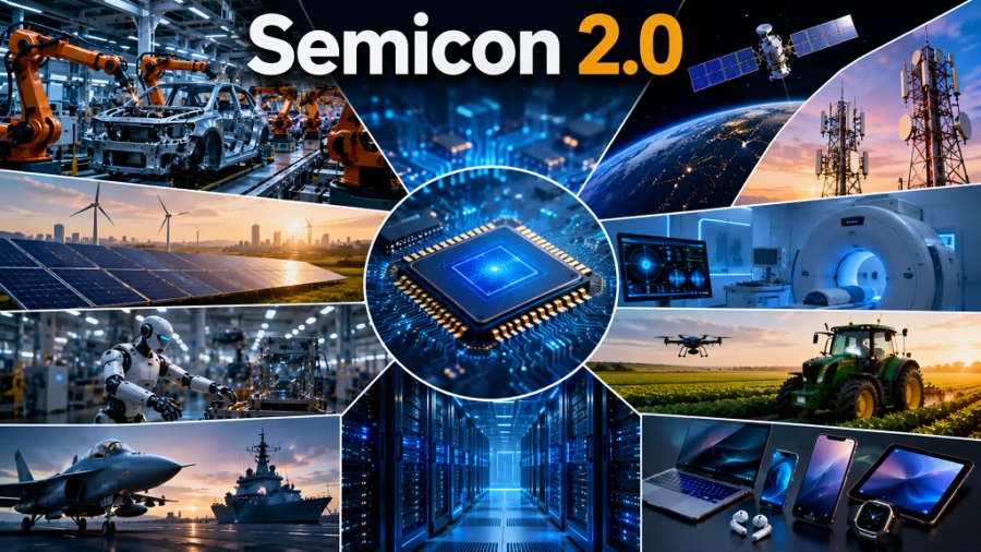
- Development of Major Industries: With an efficient semiconductor industry in place, the defence industry, the space industry, the healthcare industry, the telecom industry, the artificial intelligence industry, and the electric vehicle industry would get a continuous supply of advanced chips.
- Global Competitive Edge: Semicon 2.0 would help India enter the global semiconductor value chain because of state-of-the-art infrastructure, high-end manufacturing facilities, and a reliable international partnership.
FAQs-
A. India’s second attempt to develop the country’s semiconductor industry is called Semicon 2.0 and officially called India Semiconductor Mission (ISM) 2.0. The central government is investing ₹1.27 lakh crore in the 12 projects, which intend to create a semiconductor ecosystem with an innovative production approach.
A. While Semicon 1.0 primarily focused on manufacturing and packaging of semiconductors, Semicon 2.0 broadened its horizon to cover semiconductor equipment, materials, design, research and development, logistics, and human resource development.
A. The Six Pillars of Semicon 2.0 include:
Wafer Fabrication (semiconductor fabs)
Assembly, Testing, Marking & Packaging (ATMP/OSAT)
Ecosystem of Semiconductor Equipment & Materials
Chip Design & Indigenous IP
Research, Development & Innovation
Talented Workforce & Resilient Supply Chains
A. Industries that will benefit from Semicon 2.0 include consumer electronics, automotive, electric vehicles, telecommunications, artificial intelligence, healthcare, defence, aerospace, industrial automation, Internet of Things (IoT), and space technology.
A. The theme of Semicon India 2026 is to unite global players in the semiconductor industry under the topic “Building Trusted and Resilient Semiconductor Ecosystems.”
A. technologies that Semicon 2.0 will support include Artificial Intelligence (AI), Internet of Things (IoT), 5G/6G communication, Electric Vehicles (EV), quantum computing, robotics, aerospace, defence electronics, computing, and intelligent manufacturing.